A new, modular 128x100G building block
Next, we designed the building block switch that is at the core of all these new topologies. When designing both the topologies and the new switches, power reduction was a consideration, as well as flexibility and modularity. We wanted a single switch that would fulfill multiple roles in the data center (fabric, spine, aggregator) and also allow us to easily upgrade the network to faster optics as they become available.
With the advent of 12.8T switch ASICs, we designed Minipack, a 128x100GE switch, with a single 12.8T ASIC, instead of the 12-chip folded Clos fabric that Backpack was built upon. Using a single ASIC already brings significant power savings compared with Backpack. We worked with Edgecore to build Minipack based on our designs.
Modularity
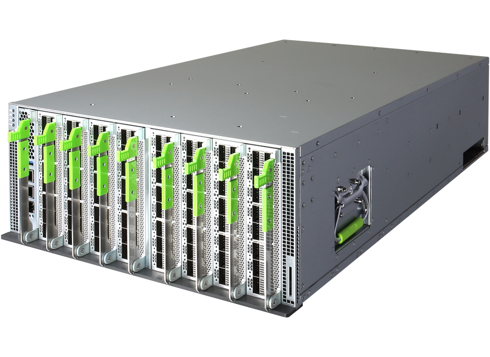
Even though we wanted a single ASIC switch, we still needed the modularity and flexibility that a chassis switch such as Backpack provides. Thus, Minipack has interface modules for the 128 ports instead of a fixed “pizza box” design. This design allows us to have both the simplicity and power savings of a single-ASIC design and the flexibility/modularity of a chassis switch.
We explored different system design options to achieve this modularity. We chose the eight port interface module (PIM) orthogonal-direct architecture because it offers the right granularity to make Minipack deployment more efficient at multiple roles in the F16 network. Each PIM card is vertically oriented in the chassis, and we overcame mechanical challenges to fit 16x100G QSFP28 ports on its front panel. We also came up with a solution to manage and route the fiber with the vertical PIMs. There are 4x reverse gearbox chips on the PIM, called PIM-16Q. When we configure the reverse gearboxes to 200G retimer mode, PIM-16Q can support 8x200G QSFP56 ports. The remaining eight ports will be nonfunctional in the 200G mode. In addition, PIM-16Q is backward compatible to 40G and supports 16x 40G QSFP+ ports. We also designed a 400G PIM called PIM-4DD, and it supports 4x400G QSFP-DD ports. Each PIM-4DD has 4x400G retimer chips. We can mix and match PIM-16Q and PIM-4DD in the same Minipack chassis to have 40G, 100G, 200G, and 400G ports.
This PIM-port flexibility allows Minipack to support multiple generations of link speeds and data center topologies, and enables the network to upgrade from one speed generation to the next smoothly.
Optics
In order to leverage the mature 100G CWDM4-OCP optics, Minipack uses reverse gearboxes. The Broadcom TH3 switch ASIC has 256 lanes of 50G PAM4 SerDes to achieve 12.8T switching bandwidth, whereas the existing 100G CWDM4 optics come with four lanes of 25G NRZ SerDes. We use reverse gearbox chips in between to bridge the gap. There are a total of 32 reverse gearbox chips in Minipack (128x100G configuration), and each processes 4x100G ports.
System design
TH3 sits on the horizontal switch main board (SMB), with a radiatorlike highly efficient heatsink, and the reverse gearboxes are on the vertical PIMs. This architecture opens up the air channel and reduces system impedance for better thermal efficiency. We can use 55-degree Celsius rated 100G CWDM4-Lite optics in Minipack while running the cooling fans at low speeds. The direct connection between SMB and PIM reduces printed circuit board trace lengths and lowers channel insertion loss. FRU-able PIM enables us to explore different interface options such as PIM-16Q and PIM-4DD, and FRU-able SCM (switch control module) improves serviceability when a dual in-line memory module or solid state disk replacement is required.
Unlike previous generations of Facebook switches, Minipack includes digital optics monitoring (DOM) acceleration function. There is one input/output block (IOB) FPGA on SMB and it is connected to the CPU by a peripheral component interconnect express (PCIe) link. The IOB FPGA talks to a DOM FPGA on each PIM through a local bus. DOM FPGA periodically polls the optics modules for DOM information through the low-speed I2C buses, and the CPU only needs to read such information from the FPGAs through the high-speed PCIe link (and avoids doing direct I2C bus accesses).
Please refer to below link for the full article: https://code.fb.com/data-center-engineering/f16-minipack/